


















































































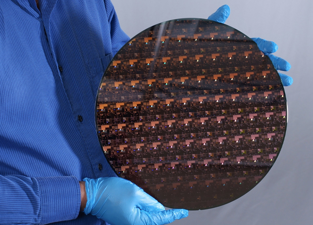
IBM unveiled a breakthrough in semiconductor design and process with the development of the world’s first chip announced with 2 nanometer (nm) nanosheet technology. Semiconductors play critical roles in everything from computing, to appliances, to communication devices, transportation systems, and critical infrastructure.
Demand for increased chip performance and energy efficiency continues to rise, especially in the era of hybrid cloud, AI, and the Internet of Things. IBM’s new 2 nm chip technology helps advance the state-of-the-art in the semiconductor industry, addressing this growing demand. It is projected to achieve 45 percent higher performance, or 75 percent lower energy use, than today’s most advanced 7 nm node chips.
The potential benefits of these advanced 2 nm chips could include:
- Quadrupling cell phone battery life, only requiring users to charge their devices every four daysii.
- Slashing the carbon footprint of data centers, which account for one percent of global energy useiii. Changing all of their servers to 2 nm-based processors could potentially reduce that number significantly.
- Drastically speeding up a laptop’s functions, ranging from quicker processing in applications, to assisting in language translation more easily, to faster internet access.
- Contributing to faster object detection and reaction time in autonomous vehicles like self-driving cars.
“The IBM innovation reflected in this new 2 nm chip is essential to the entire semiconductor and IT industry,” said Darío Gil, SVP and Director of IBM Research. “It is the product of IBM’s approach of taking on hard tech challenges and a demonstration of how breakthroughs can result from sustained investments and a collaborative R&D ecosystem approach.”
IBM at the forefront of semiconductor innovation
This latest breakthrough builds on decades of IBM leadership in semiconductor innovation. The company’s semiconductor development efforts are based at its research lab located at the Albany Nanotech Complex in Albany, NY, where IBM scientists work in close collaboration with public and private sector partners to push the boundaries of logic scaling and semiconductor capabilities.
This collaborative approach to innovation makes IBM Research Albany a world-leading ecosystem for semiconductor research and creates a strong innovation pipeline, helping to address manufacturing demands and accelerate the growth of the global chip industry.
IBM’s legacy of semiconductor breakthroughs also includes the first implementation of 7 nm and 5 nm process technologies, single cell DRAM, the Dennard Scaling Laws, chemically amplified photoresists, copper interconnect wiring, Silicon on Insulator technology, multi core microprocessors, High-k gate dielectrics, embedded DRAM, and 3D chip stacking. IBM’s first commercialized offering including IBM Research 7 nm advancements will debut later this year in IBM POWER10-based IBM Power Systems.
50 billion transistors on a fingernail-sized chip
Increasing the number of transistors per chip can make them smaller, faster, more reliable, and more efficient. The 2 nm design demonstrates the advanced scaling of semiconductors using IBM’s nanosheet technology. Its architecture is an industry first. Developed less than four years after IBM announced its milestone 5 nm design, this latest breakthrough will allow the 2 nm chip to fit up to 50 billion transistors on a chip the size of a fingernail.
More transistors on a chip also means processor designers have more options to infuse core-level innovations to improve capabilities for leading edge workloads like AI and cloud computing, as well as new pathways for hardware-enforced security and encryption. IBM is already implementing other innovative core-level enhancements in the latest generations of IBM hardware, like IBM POWER10 and IBM z15.